Research

Projects
Most images can be clicked to view larger version.
Project 1: Lab on CMOS Systems
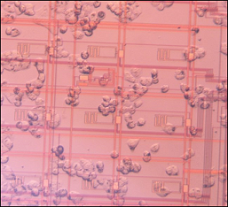
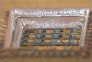
Lab-on-CMOS (LoCMOS) devices are microsystems incorporating one or more CMOS chips that are designed to perform laboratory functions directly on the surface of the chips, allowing for intimate contact between sensing inputs and the cells under analysis. Lab-on-chip devices integrate multiple laboratory functions into a single device, but usually incorporate a passive sensing layer that requires external instrumentation for readout and signal processing. Integrating active chips into lab-on-chip systems provides the opportunity for sensing and actuation in intimate contact with readout and electronics, producing systems with smaller size, higher sensing density, higher sensing fidelity, and novel capabilities. Prof. Abshire and colleagues are currently pursuing several applications of this technology including a “nose on a chip” olfactory sensor, implantable diagnostic devices for cancer, and a neural computation platform.
Project 2: Adaptive Integrated Circuits
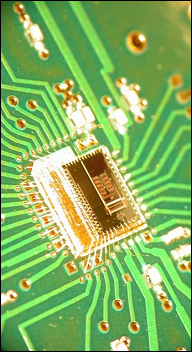
The Adaptive Floating Gate Comparator is a flash ADC comprising an array of high speed adaptive floating gate comparators. On-line learning enables manual and automatic in-circuit programming of reference levels, eliminating comparator offset and enabling advanced functionality such as histogram equalization. Prof. Abshire has introduced methods for designing adaptive circuits that use local autonomous tuning and storage to overcome component mismatch and improve performance for a variety of applications, including imagers, adaptive filters, comparators, analog-to-digital converters, cell-substrate capacitance sensors, true random number generators (tRNG), visual motion sensors, low light sensors, and analog computation. Adaptive approaches can minimize power-hungry processing for systems operating under extreme size-weight-power (SWAP) constraints. In applications such as the tRNG and CTIA-based low light sensor, adaptive approaches enhance performance by achieving tight, low level tuning of a physical mechanism.
Project 3: Cell Capacitance Sensors
Living cells are capacitively coupled to their underlying substrate, a phenomenon responsible for on-chip capacitance sensing of cell viability. Prof. Abshire and her students were the first to propose, design, and demonstrate cell-substrate capacitance sensors which track the cell-substrate interaction process by measuring the capacitive coupling between cells and their substrate in the presence of weak electric fields. Recent generations of this suite of sensors have been extended to include digital readout using an I2C bus and to function as peripherals to commercial microcontrollers; they provide an electronic analogue for cell health, a critical sensor modality in understanding cell biology and disease. She and her students have demonstrated that these measurements correlate with the behavior of individual cultured cells and can detect events such as cell adhesion, migration, mitosis, and death.
Project 4: CMOS Contact Imager
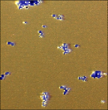
Contact imaging is an imaging configuration in which the sample is in close proximity to the sensor surface without the use of an intermediate lens. In LoCMOS biosystems, the sample comprises cells which are located on the sensor surface. To detect absorption, standard farfield illumination is applied, and the cells in between the light source and the sensor surface block light; thus, the locations of the cells are represented by dark pixels in the image. Prof. Abshire and her students were the first to characterize the resolution and contrast of CMOS contact imaging, demonstrating that contact imaging can be used to observe biological cells and small particles nearby the sensor surface.
Project 5: Nose on a chip
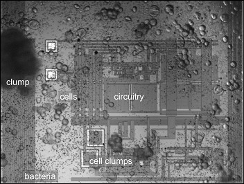
On-chip sensing of physical signals is now relatively straightforward, with accelerometers and cameras now ubiquitous, but sensing of odorants has proven to be far more challenging. In collaboration with Elisabeth Smela (ME) and Ricardo Araneda (Biology), Prof. Abshire has developed and demonstrated a nose on a chip olfactory sensor, using the electrical activity of olfactory sensory neurons cultured on integrated circuit chips to detect odorants. Biological olfactory sensors have, as yet, no equal in human-made devices.
Project 6: Redox Actuation on Chip
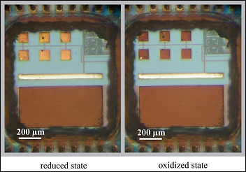
Hybrid LoCMOS/MEMS microsystems enable high-speed, automated and economical cell monitoring for various applications including studies of specific biochemical mechanisms, fast medical diagnosis, pharmaceutical tests, and biochemical detection. In collaboration with Elisabeth Smela (ME). Prof. Abshire developed and demonstrated the first CMOS potentiostat with on-chip electrochemical actuation. The integrated potentiostat comprises CMOS control circuitry connected to microelectrodes that constitute the on-chip electrochemical cell. The potentiostat module has been successfully tested for in situ deposition and control of PPy films on the on-chip electrodes. The electrochemical actuation causes the Ppy films to change color.
Project 7: Odor Sniffing Nano Quadcopter
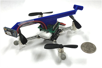 Profs. Abshire and Horiuchi have developed a nano-quadcopter system that performs odor detection in a windless indoor environment. The system uses the Crazyflie platform and incorporates a single commercially available metal oxide semiconductor gas sensor. They have demonstrated that rotor-induced airflow enhances odor detection with minimal power consumption and can be considered to be the quadrotor equivalent of sniffing behavior.
Projects
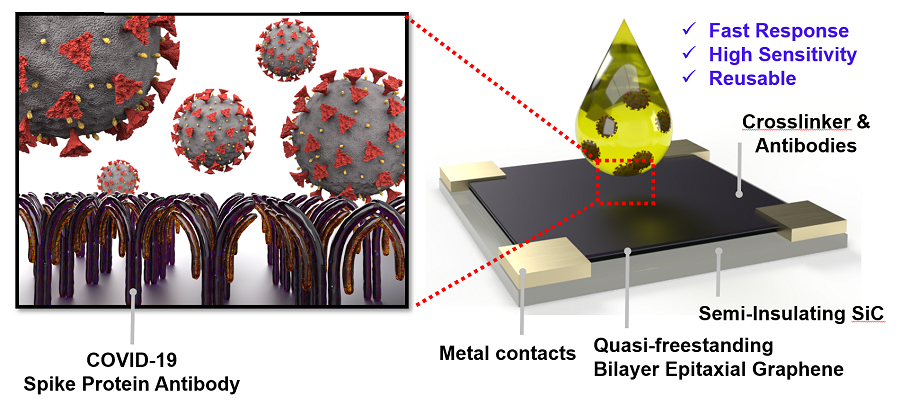
Project 1: Fast electrical detection of SARS-CoV by spike protein antibodies immobilized on epitaxial graphene on silicon carbide.
Project 2: Fast response/recovery time, nitrogen selective gas sensor using 2D manganese dioxide epitaxial graphene heterostructures.

Projects
<br “clear=all”>Project 1: Integrated Capsule Microsystems for in situ Biosensing and Diagnostics
Integrated Capsule Microsystems for in situ Biosensing and Diagnostics
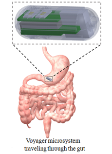
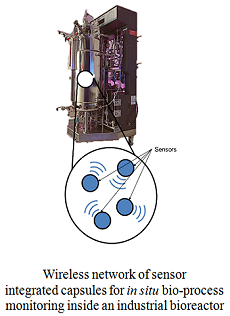
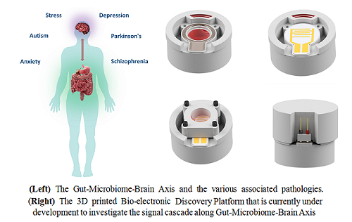
With the advancement of micro- and nano-technologies, miniaturized bio/medical devices and systems are becoming increasingly more viable for addressing challenges associated with the current state-of-the-art methodologies, which require complicated and expensive devices manned by trained personnel. Our group is taking a multi-directional approach developing smart miniaturized bio/chemical sensing platforms for in vivo diagnostics of GI tract, real-time monitoring of biological reactors and unveiling molecular cross talk occurring at the gut-microbiome-brain-axis. Electrochemical detection, is a simple yet powerful tool for molecular and cellular biosensing in aqueous environments. By encapsulating electrochemical electrodes along with battery and communications electronics, we aim to send these capsule type devices into biological environments (e.g. GI tract) where they can wirelessly transmit molecule biosensing data for external analysis toward better pancreatic adenocarcinoma (PA) diagnostics. We aim to develop capsules capable of detecting digestive enzymes and microRNA, characteristic of PA in pancreatic secretions present in the GI tract. To achieve this, we are integrating biomarker-specific sensors with off-the-shelf microelectronics, packaged within a 3D-printed capsule to protect our system while it wirelessly transmits signals to a mobile phone. Our long-term goal is to utilize this device as a preemptive screening tool for patients with potential for developing PA. This microsystem has the potential to be customized to sense and transfer useful diagnostic data on various events occurring in the gut. A larger scale version of an analogous system can be used to monitor the distribution of molecules of interest in a bioreactor. At these scales, it is critical to understand the biochemical profile of the environment. This tool will introduce a new level of sampling and quality control to various industrial bioreactor systems. A similar electrochemical sensing approach is also being used to design a lab-on-a-chip in vitro model of the gut, with integrated porous Impedimetric and electrochemical sensors for evaluating one’s gut-microbiome. This device would be used to diagnose the metabolic state of the gut microbiome in patients exhibiting both GI and neurological disorders and solve the missing links in molecular cross talk at the Gut-microbiome-brain-axis.
Project 2: Micro-Nano-Bio-Systems Integration Using Biological Nanoscaffold for Sensing and Energy Harvesting
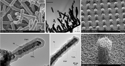 Electron microscopic images of nanostructured energy storage electrodes created via integration of TMV nanoscaffolda with advanced micro/nanofabrication technologies.
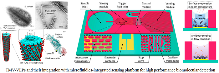
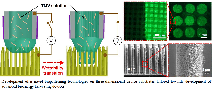
The convergence between biochemistry and micro/nano manufacturing technologies has led to revolutionary advancements in the development of miniaturized devices and systems equipped with biochemical functions from integrated biomaterials (e.g. nucleic acids, antibodies, viruses, etc.). Particularly, viral nanoparticles that are non-infectious to humans (plant viruses and bacteriophages) have been vastly utilized as functional nanomaterials leveraging their self-assembled nanostructures, molecular storage functions, and high-density protein residues expressed on their surface. Over the past decade, the efforts by our group and collaborators have focused on combining genetic-engineering and microfabrication/MEMS technologies to unveil beneficial utilities of a specific plant virus, tobacco mosaic virus (TMV), and its gene-free derivative, virus-like-particles (VLPs), for developing a range of advanced nanomaterials and microsystems. TMV displays a cylindrical high-aspect-ratio structure formed by assembly of thousands of identical CPs encapsulating its genome. The bio-nanoscaffold serves as an excellent building block for synthesis/fabrication of nanomaterials for a range of applications including high performance charge storage devices (e.g. Li-ion batteries, supercapacitors) and superhydrophobic surface coatings. In addition, the naturally arranged high density surface receptors can offer versatile functions for developing advanced bioelectronics including bio/chemical sensors and bioenergy harvesting devices. We continue our efforts in developing methodologies to overcome fundamental challenges associated with integration of TMV/VLP particles with micro/nano devices, with the long-term aim of developing translational microsystems enabled by harmonic hybridization of bio-, nano-, and micro- components.
Project 3: Micro/Nano Devices and Systems for Bacterial Biofilm Detection, Monitoring and Inhibition
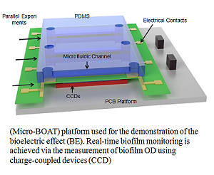
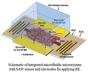
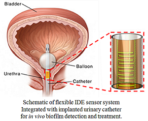
Microsystems with integrated biosensors are making a paradigm shift in the way biomedical devices are impacting the field of health care. Biofilms are ubiquitous in healthcare and is a leading cause of hospital associated infections (HAIs) causing catheter and implant associated infections. Biofilm consists of cells encased in a sticky polysaccharide extracellular matrix, forming when bacteria adhere to hydrated surfaces. Traditional research has focused on planktonic bacteria when developing therapies for treating infections. However in reality, biofilms provide bacteria with elevated resistance to traditional antibiotics, rendering these treatments ineffective. Furthermore, biofilms and the higher doses of antibiotics used for treatment serve to exacerbate the spread of antibiotic resistance. In our group, we have developed several microsystems for effectively characterizing and treating biofilms. Microfluidic systems enable tight control of the biofilm microenvironment and minimize reagent volumes, allowing rapid high-throughput testing of the interactions of different compounds and conditions with biofilm. Also, these microfluidic systems can be designed with integrated controls to improve experiment reproducibility and minimize the impact of the inherent variability in biofilm growth. In addition, we have developed integrated microsystems combining the microfluidics with novel biofilm sensing and treating strategies. In particular, our recent efforts have demonstrated real-time monitoring of biofilm growth by measuring the biofilm-induced change in biomass or dielectric property using surface acoustic wave sensor or an impedance sensor. In addition, these sensors have been integrated with a biofilm removal mechanism, bioelectric effect, a phenomenon where a small electric field increases the susceptibility of a biofilm to an antimicrobial compound. Our current efforts are tailored towards developing flexible sensing platforms to allow the integration of these sensing and treating systems with the complex geometries of relevant colonized surfaces in medical applications. Overall, the developed microsystems will allow us to examine novel treatment methods and minimize the spread of antibiotic resistant strains which would make a significant impact in healthcare.
Projects
Project 1: Semiconductor Physics: Devices, Materials and Circuits:
A good deal of Prof. Goldsman’s research is focused on the physics and computer aided design for semiconductor materials, devices and circuits. To model, design and analyze new semiconductor devices and materials we have a comprehensive suite of CAD codes. Most of these codes have been developed in-house by Prof. Goldsman’s research group, while some have been adopted from the public domain and have been adapted for modeling semiconductor devices and materials. Prof. Goldsman’s group uses these codes and regularly updates them to design new devices, circuits and materials, and to theoretically investigate the physical origins of semiconductor phenomena. The following CAD tools are a key component of research and design for nanoelectronics:
Project 2: 2-Dimensional Device Simulation
Is the workhorse of device modeling. Here the system of coupled partial differential Semiconductor Equations are solved numerically self consistently to provide details inside the device including the electron and hole concentrations, current densities and electrical potential, as well as how the I-V characteristics depend on the device design.
Project 3: Monte Carlo Simulator
Models electron and hole transport on the atomic level. It is vital for understanding how to improve carrier mobility and thus the performance and operational speed of devices.
Project 4: Electronic Energy Band-Structure Solver
The energy band structure contains most of the electronic properties of a material, This CAD calculates the bands structure of virtually any semiconductor, and then uses it to model mobility, scattering and optical properties of the material.
Project 5: Density Functional Theory (DFT) Quantum Many-Body Solver
Calculates how defects effect material and devices properties. It is a powerful tool that provides detailed information how atom-by-atom engineering of materials can be used to develop new electronic materials and devices.
 Process Simulation: Semiconductor devices are fabricated through a very complicated set of processes that include nanoscale photolithography, oxidation, ion-implantation, chemical etching, electron-beam deposition, atomic sputtering, atomic layer deposition, etc. Modeling of these processes is assiduously performed before committing to actual fabrication.
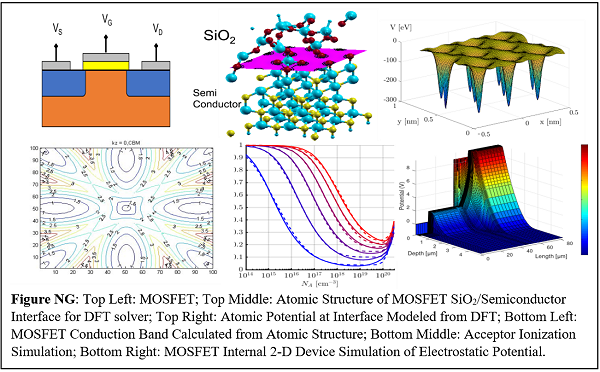
Figure NG shows some example CAD steps that we can go into the design and fabrication of a MOSFET. Along the top row of the figure, the cross-sectional MOSFET diagram is shown, next to that is the atomic structure of the MOSFET Oxide-Semiconductor Interface that goes into the DFT calculations. The atomic potential of the interface atoms is on the right which is one of the outputs of the DFT. The bottom row shows the result of the energy band calculator giving great details of the semiconductor conduction band in k-space. In the middle is the simulated ionization of acceptor atoms versus doping concentration and temperature. Finally, on the bottom right is the internal electrostatic potential inside a MOSFET. Many calculations of this type are performed to design the optimal transistor before the factory commits to fabrication, which can cost many millions of dollars.
Projects
Note: You can click on the images to view the larger version.
Project 1: Neuromorphic VLSI Spiking Neural Network Models for Negotiating Obstacle Fields
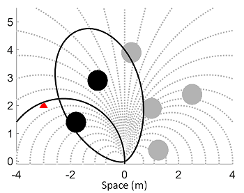 The ability to quickly scan an area for obstacles and rapidly make decisions about the direction of travel is critical for a flying animal such as an echolocating bat. When the sonar beam is narrow (as it is in our artificial system), head turning and sensory memory is important to good decision making. In this research, we are developing a detailed spiking neural model for rapidly guiding the orientation of a narrow field-of-view sonar sensor, combining sensor data from sequential sonar pings, and selecting travel trajectories, all while heading towards a goal. This research involves algorithmic simulations of an echolocating bat in a simulated world of trees, mobile robots carrying sonars, and neuromorphic VLSI spiking neural networks for low-power, real-time implementation.
Project 2: Echolocation-Based Place Recognition
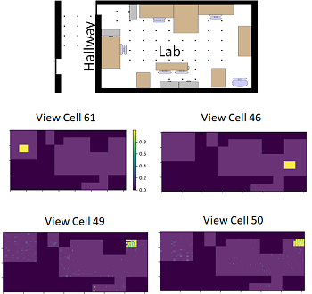
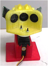 The memory and recognition of previously-visited locations is a critical capacity to support Place Recognition mapping and route planning in creatures big and small. To explore and understand these behaviors in artificial bat-like systems, we have been developing neural models for echolocation-based place recognition. In this research, we have been using artificial neural network models to recognize the complex echo patterns from different locations in our laboratory environment. While similar research efforts seek to reconstruct tight position coordinates (like GPS), we are more interested in modeling the recognition of a broad region of space similar to what is observed in ‘place cells’ of the mammalian hippocampal brain areas.
Project 3: Counter-sUAS Interceptor Drone Project
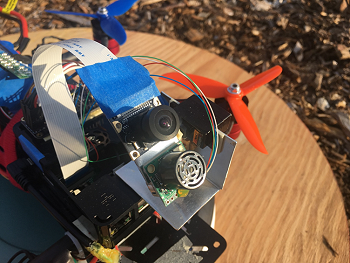
To address the growing problem of small unmanned aircraft systems (sUAS) entering an airspace without authorization over a public event, building, or other protected spaces (whether for recreational purposes or with malicious intent), we have been exploring the use of a low-cost, aerial intercept vehicle that can autonomously pursue a targeted sUAS in the sky and launches a propeller entanglement device to bring it to the ground. An intercept vehicle based on a small racing quadcopter is guided by a visible-light camera and sonar to attack the target sUAS from below. Our guidance approach is inspired by animal models such as the echolocating bat and the dragonfly.
Projects
Project 1: Remote RF IC Sensors for RF Tracking
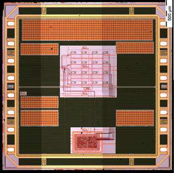
Development of CMOS IC of RF sensor chip capable of tracking RF remote emissions. The design and development of the chip circuit design is realized in 180nm CMOS technology and uses a tracking algorithm, on-chip patch or external antennas, optimized low noise amplifiers, and an innovative front end Gilbert cell multiplier.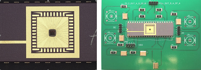
Fig. 1. Packaged chip and custom designed PC board for mounting and testing the RF sensor chip. Jooik Chung and A. A. Iliadis.
Project 2: Development of Betavoltaic Power Cells
Betavoltaic power cells are promising long time (>10 years) continuous production of power for applications in the medical field such as heart pacers, sensors, and space. The project deals with the development and optimization of betavoltaics in GaN and Si, targeting to optimize and increase power output under beta irradiation.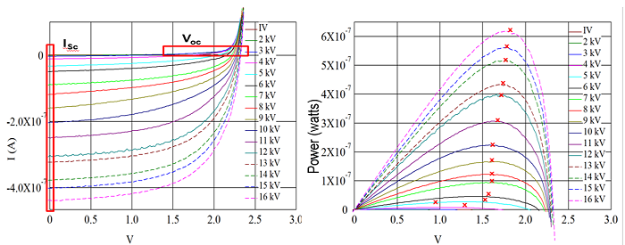
Fig. 2. I-V characteristics and P-V curves for various beta irradiation energies for a GaN diode.
Project 3: Nano-ZnO/Si Heterojunction pn Diode Field-Assisted Gas Sensors
N type ZnO self assembled nanostructures on p type Si wafers formed an effective pn heterojunction diode with with extended surface suitable for gas sensing applications with high sensitivity and responsivity at room temperature. In addition to the extended surface for sensing, the field assisted gas sensing provides an additional process in the sensing mechanism, whereby the sensing becomes more efficient and rapid, by introducing the nano p-n junction close to the surface in order to enhance sensitivity and responsivity of the sensor. Sensing of H2 gas is shown in the figures below.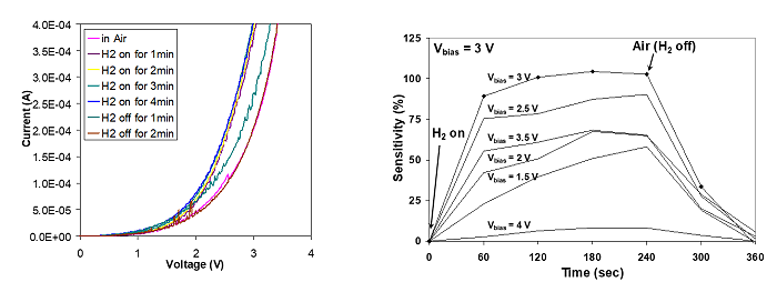
Fig. 3. A. Current -Voltage (IV) characteristics of the nano-sensor. B. Sensitivity vs time under different forward bias points for the nanodiode. Optimal sensing is for a bias point of 3.5V.
Projects
Prof. Khaligh’s major research interests include modeling, analysis, design, and control of power electronic converters for transportation electrification, renewable energy and wearable electronics.
Recent projects include:
Project 1:
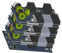
Design and development of a modular GaN regulated transformer rectifier unit (RTRU), with power density of 1.2 kW/liter, specific power of 1.76 kW/kg, and peak efficiency of more than 96%. This is the first fully GaN-based AC-DC converter for aircraft (possibly any) applications, through support from Boeing Company.
Project 2:
Holistic microinverter design approach, considering both converter- and system-level perspectives, to reduce the levelized cost of energy (LCOE) for residential microinverters. Specific objectives and outcomes include a low bill of material cost (< 7 ¢/W), high efficiency (> 97%), high power density (> 3.3kW/Liter), and high reliability (> 250,000 hours mean-time-to-failure, MTTF), in collaboration with Enphase Energy through a $2.37M award from DOE.
Project 3:
A thermally-Integrated high power density isolated dc/dc converter with additive manufacturing using bare-die SiC switches. This project utilizes multi-functional elements, serving simultaneously as electrical bus-bars as well as heat sinks and an innovative way for double-sided cooling to improve electro-thermal performance. A 10 kW bidirectional isolated dc-dc converter is designed with power-density of 10.8 kW/liter and max efficiency of 97%.
Projects
The research focus of our lab is to investigate circuits, systems and novel architectures to compute efficiently in a resource constraint environment (wearable, implantable, and edge devices). Specific focus is on investigating and developing integrated CMOS based systems that can lead to low-power consumption while processing signals in real-time. Our research also includes investigating novel computing architectures such as neuromorphic computation.
Research projects include:
Project 1: Bidirectional brain-machine interface
Project 2: Continuous physiological monitoring
Project 3: CMOS based bio-sensing
Project 4: Edge devices for embedded machine learning
Note: You can click on the images to view the larger version.
Projects
Project 1: Magnetic Fields for Head
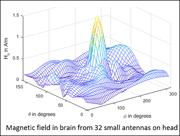
In order to avoid drilling holes in the head for probes to stop Parkinson’s disease tremors, this research is for the design of multiple small antennas on a helmet allowing for creation of a steerable magnetic field. This allows excitation or extinction of neural activity excited by the presently used probes. The fields have been designed by research with Professor Mohammad Safar of Kuwait University.
Project 2 : Neural Type Cell Circuits2.
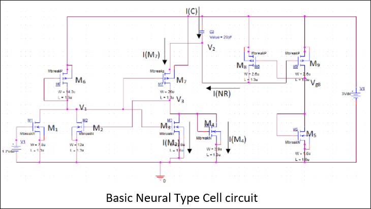
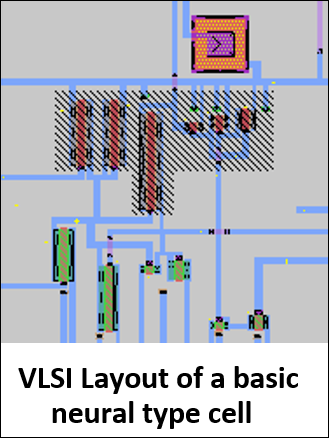
This research is for the design of VLSI circuits which mimic the pulsing behavior of biological neurons, not by simulating their equations but by mimicking their function. It involves the transistorized design of hysteresis oscillators with the latest student layouts by students for 180nm fabrications. This research originated with a joint US-State Department grant with Professor Michel Bialko of Gdansk Technical University, Poland.
Project 3: Scattering Matrix, Active Synthesis
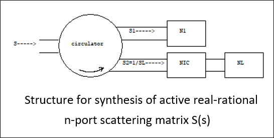
The synthesis of finite dimensional passive circuits proceeds from bounded real (=BR) scattering matrices. Extending these ideas, that for single port active circuits can proceed from a method of Wohlers using negative impedance converters to invert scattering matrices. This research extends active circuit synthesis to any finite dimensional scattering matrix and can lead to its VLSI realization.
Project 4: N-Grains Simulation
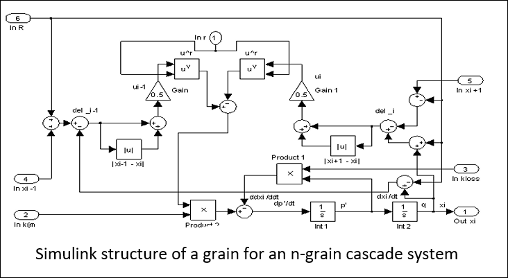
The theory of grains proceeds from partial differential equations described by 3/2 power forces and allows for soliton-like waves. The ideas could possibly lead to soliton multi-computers. To construct finite circuits, the grain systems can be discretized as shown in the figure for one section allowing for Simulink simulation. This research is joint with Professor Surajit Sen of SUNY, Buffalo.
Project 5: Neurotechnology Research
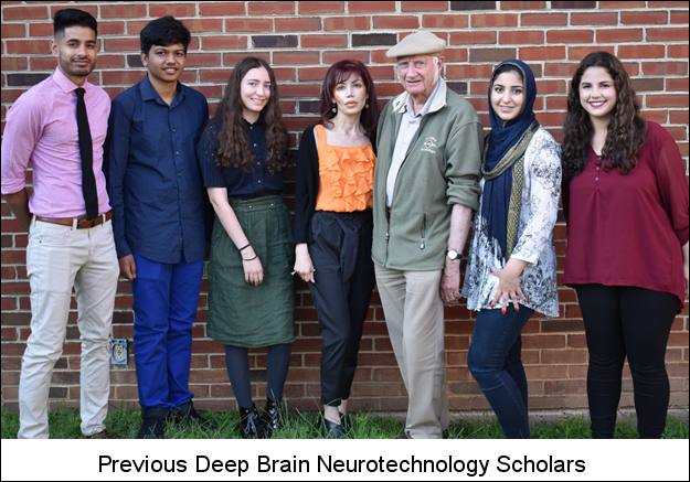
Under the UMD freshman research program, FIRE, this mentored research has been headed by Dr. Nevine El-Leithy and has pursued such topics as 3D printing of a magnetic steering helmet and mapping of the brain via the computer simulation program MIDAS in conjunction with FDA researchers.
Projects
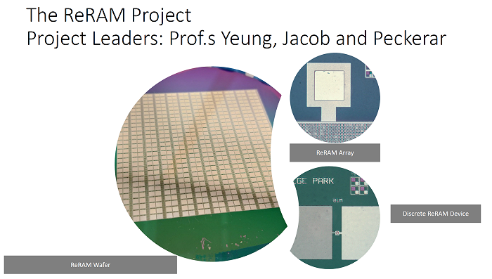
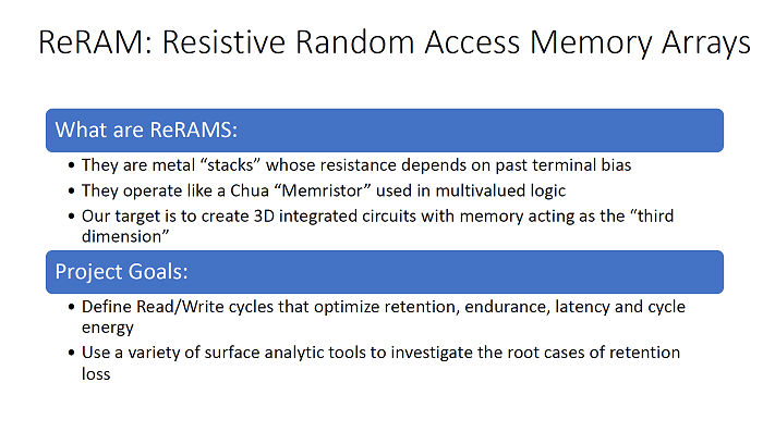
Project 1: ReRAM
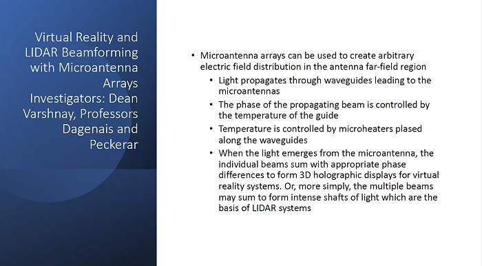
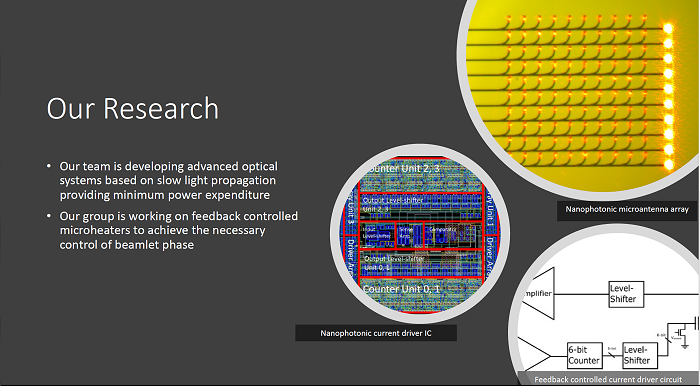
Project 2: Virtual Reality and LIDAR Beamforming with Microantenna Arrays
Projects
Maryland Shaping Energy and Minds (M-SEM) lab is striving to provide the proper energy and power for any applications that require energy and power, considering factors such as proper waveforms, time, amount, amplitude, polarity, frequency, size, position, cost, and e.t.c.. These efforts may involve materials, electronics, power, control, and electromagnetics. Currently, we are focusing on
Project 1: 3 – 300 MHz Power Conversion and Wireless Transmission, especially for wireless power transfer and plasma generation.
Project 2: Pulse Power Electronics, including high electric field, high magnetic field, high current, and high voltage generation and distribution.

